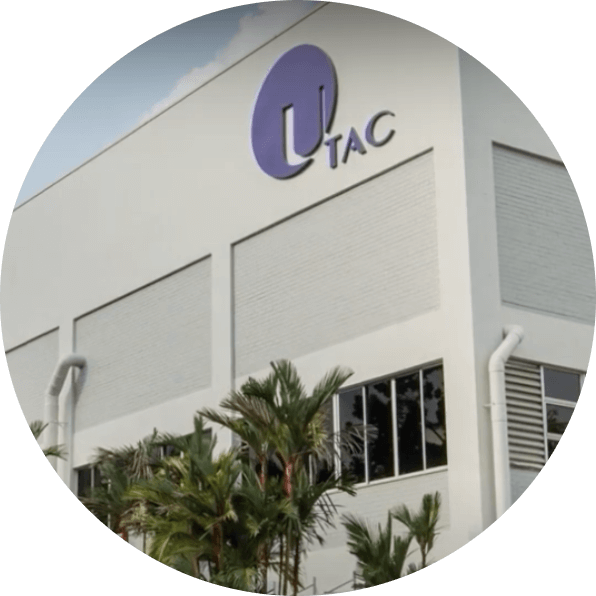
As a global leader in outsourced semiconductor assembly and test (OSAT) services, UTAC delivers advanced semiconductor packaging and testing solutions from strategic locations in Singapore, Thailand, Indonesia, and China. With expertise in automotive semiconductor solutions, secure intellectual property (IP) protection, and a foundation of geopolitical stability, UTAC is the partner of choice for mission-critical applications in automotive, computing, and communications markets.
From design to production, we enable reliable and scalable semiconductor technologies.
UTAC delivers end-to-end semiconductor assembly and test solutions optimized for performance, size, and power efficiency.
From wafer probing to final testing, we provide comprehensive manufacturing capabilities spanning wafer-level packaging, laminate packages, leadframe solutions, SiP integration, MEMS & sensors, and power applications. Our precision engineering and seamless integration processes are backed by advanced quality systems and proven automotive expertise.
Our flexible business model adapts to customer requirements through:

GREEN ENERGY
Greenhouse Gas Emissions
Established and continually enhanced the measurement and tracking of Scope 1 and 2 emissions to achieve better data quality
In the progress of developing our Scope 3 emissions inventory

SAFETY
Maintained our record of zero fatalities
Received the Gold Class Award in Zero Accident Campaign for the 4th consecutive year in Thailand
Diversity and Inclusion
Community Impact

Sustainable Supply Chain
Customer Satisfaction

Catch up on our latest announcements, partnerships, and breakthroughs.
Explore press releases and event schedules to learn more about UTAC Group and connect with us at global industry events.
Stay ahead with insights and innovations from UTAC Group
Access white papers and technical briefs on the latest industry challenges and opportunities in semiconductor technology from UTAC Group experts.


