UTAC has in-house Failure Analysis (FA) lab in every factory to provide quick turn-around time for physical FA (PFA) and Electrical FA (EFA) for IC packages, modules and PCB boards.
At UTAC, our quality organization is centralized, our QA engineers can seamlessly leverage laboratories/resources across multiple UTAC sites (if needed) allowing customers to take their products to market as quickly as possible.
FA lab supported by team of more than 10 engineers and technicians with average experience of more than 10 years.
Capabilities augmented by link-up with local analysis labs to provide services such as Focused Ion Beam (FIB) and Transmission Electron Microscopy (TEM).

Test Types
Click any of the services below to learn more. Click the arrows on the right to view more services.


Curve Trace
Technique:
Curve Trace
Application:
Curve Tracing is used to verify and confirm electrical failures that exhibit abnormal current-voltage (IV) characteristics at the device function pins. Open connections, short circuits and other DC characteristics are investigated usually by comparison with a known good device. A curve tracer is used with two probes, one for each of the nodes that define the electrical path being characterized.

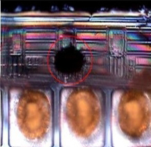
X-ray Radiography
Technique:
X-ray Radiography
Application:
X-ray Radiography is a nondestructive failure analysis technique used to examine the interior details of the package. X-ray inspection uses the fact that X-ray penetration varies according to the type of material and thickness. The device is subjected to penetrating X-rays and a resulting image is produced on a photographic film or on a screen (for real time X-ray). The recorded radiograph is a shadow image which shows the differences in density brought about by internal material variations in the device under observation. This method is effective for detecting interconnect defects, die attach voids, package voids and cracks inside the plastic sealed package

Scanning Acoustic Microscopy
Technique:
Scanning Acoustic Microscopy (SAM)
Application:
Scanning Acoustic Tomography is a non-destructive failure analysis technique which uses high frequency ultrasonic energy to image internal features, characterize material properties and detect defects via an acoustic wave. It is used for detecting disbonds or delamination between package interfaces, voids and cracks using the pulse-echo mode (C-scan) and through transmission mode operation (Thru-scan).

Visual Inspection
Technique:
External (EVI) and Internal Visual Inspection (IVI)
Application:
Optical Microscopes are commonly classified as either low-power or high-power microscopes. Low-power microscopes are those which typically magnify the specimen at 5X to 60X, although some can magnify up to 100X. High-power microscopes typically magnify the specimen at 50X to 1000X. Visual Inspection is non-destructive in nature and is used to detect abnormality on external and internal parts of an IC.

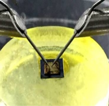
Decapsulation
Technique:
Laser Decap method
Application:
Laser Decap is a dry method of decapsulation, using a high-power laser to ablate the plastic encapsulant material away from a device. Laser decapsulation system is controlled with precision stepper motors to achieve more precise positioning than chemical etching. It is possible to decapsulate devices that would be exceptionally challenging to expose chemically (eg. Cu wire bond) and can do partial/selective decapsulation. If used in combination with chemical etching, yield rate can be greatly improved as contact time with chemicals is reduced.
Technique:
Chemical Decap method
Application:
Decapsulation is a step performed to expose the internal parts of the IC (dies and internal bonding) by removing a portion of mold compound area and depth in preparation for inspection, chemical analysis or electrical examination of the die and the internal features of the package. This is done without altering the IC’s original electrical characteristics.
Chemical Preparation
Technique:
Deprocessing / Chemical Etching / Cratering / IMC Test
Application:
Destructive Chemical Etch Methods to remove metals and other parts of an IC selectively (eg. Al bond pad layer removal, IMC exposure).
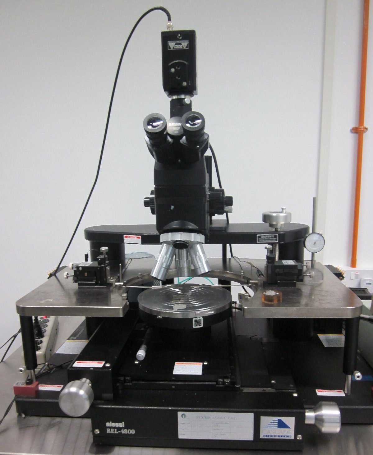
Microprobe
Technique:
Microprobe
Application:
Microprobing is a method to access defined node or section (i.e die circuit, wirebond, substrate, etc) to have electrical contact, It employs an equipment known as a microprobe station. A microprobe station consists of a microscope holder and several probe holders which can be moved in the X, Y or Z direction independently. Fine-tipped probe needles are held by the probe holders and electrical contact is made by dropping the fine-tipped probe needles directly on the point of interest, or on an area to which the point of interest is connected precisely.


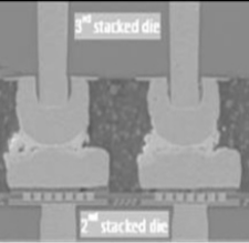
Cross-section
Technique:
Mechanical Cross-section
Application:
Cross-sectioning is a technique for mechanically exposing a plane of interest in a die or package, usually at right angles to an axis. It consists of grinding and polishing the specimen until the plane of interest is ready for optical/electron microscopy inspection or for further analysis. To avoid introducing artifact, initial preparation usually require the encapsulation of the specimen in plastic to give it stability, support & protection.
Technique:
Parallel Lap
Application:
Parallel Lapping is the removal of material precisely from a specimen to produce a smooth, flat, unpolished surface to the required thickness and flatness.
Technique:
Ion Mill
Application:
Ion milling is a physical etching technique whereby the ions of an inert gas are accelerated from a wide beam ion source and bombarded into a surface, resulting in sputtering of material from the surface. This process exposes underlying material while protecting it from mechanical stress. It is used to prepare polished cross-sectional samples prior to SEM analysis when manual mechanical polishing proves difficult.
Liquid Crystal Analysis
Technique:
Liquid Crystal Analysis (LCA)
Application:
Liquid Crystal Analysis is a failure analysis technique used to localize areas on the die surface that exhibit excessive heating. It is a simple technique to hot spot detection with good sensitivity and spatial resolution which detects tens of microwatts power dissipation (mA leakage). Excessive heating indicates a high current flow, which may be due to die defects or abnormalities like ESD/EOS damage, dielectric ruptures, metallization shorts, leaky junctions and latch-up locations.

Emission Microscopy
Technique:
Emission Microscopy (EMMI)
Application:
Emission Microscopy is an efficient failure analysis technique used to detect and localize IC failures such as gate oxide defects, ESD failure, junction leakage, latch-up, etc. EMMI consists of a highly-sensitive CCD camera capable of detecting photons emitted in the device and can be performed from either the front or back of IC devices.

Scanning Electron Microscopy
Technique:
Scanning Electron Microscopy (SEM)
Application:
Scanning Electron Microscopy is the most common and well-known electron microscopy method for the physical imaging of surfaces. The SEM is a powerful and versatile instrument both for inspection and failure analysis. It is a dynamic scanned beam imaging system as opposed to static beam imaging systems such as optical microscopes. SEM is used for inspecting topographies of specimens at very high magnifications, typically up to 30KX. SEM inspection is often used in the analysis of die or package cracks and fracture surfaces, bond failures and physical defects on the die or package surface.

Energy Dispersive X-ray
Technique:
Energy Dispersive X-ray (EDX)
Application:
Energy Dispersive X-ray Analysis is an analytical technique used for identifying the elemental composition of a specimen or an area of interest in the specimen. It is also used for elemental detection of contamination and foreign material. It is normally coupled with SEM for micro area analysis. An energetic electron beam excites the sample to emit characteristic X-rays of the elements which is used to identify and quantify the sample composition.
The output of an EDX analysis is an EDX spectrum which is just a plot of how frequently an X-ray is received for each energy level.

Fourier Transform Infrared Spectroscopy
Technique:
Fourier Transform Infrared (FTIR) Spectroscopy
Application:
Fourier Transform Infrared Spectroscopy or FTIR Analysis, is an analytical technique that uses IR light to measure chemical bonds and to identify organic materials. When IR radiation passes through a sample, some signals will be absorbed and some will pass through. The signal produced (Interferogram) will be converted through Fourier Transform into an interpretable spectrum that can be used to match through various commercially-built and in-house libraries.